
Tag: ICMAB

X-Ray Diffraction
The X-ray Diffraction Laboratory is a consolidated service of the ICMAB institute. The main objective of the service is to meet the needs of the different departments of the center offering the maximum possible benefits to the institute users and it is also available to external users.
Based on the principles of X-ray diffraction, a wealth of structural and microstructural information about crystalline materials can be derived. In materials science, knowledge of the structure and composition of the materials studied is a key requirement for understanding their properties.
Our fast, accurate and customized services include data collection, qualitative and quantitative phase analysis as well as texture measurements (pole figures), residual stress, reciprocal space maps, etc. The most common function of the service is the acquisition of X-ray diffraction data under different conditions, e.g. by using flat sample and Bragg-Brentano geometry, thin film diffraction, texture determination on layers, microdiffraction and qualitative analysis in capillary materials.

Proximity Probes
The Scanning Probe Microscopy (SPM) Lab is one of the Scientific and Technical Services at ICMAB. The service offers several AFM microsocpes for surface characterization. MFP-3D, Azylum, especially dedicated to magnetic, ferroelectric and photoelectric characterization.
The SPM Lab offers SPM related experiments both to the ICMAB community and to external users. We are open to all reserachers at ICMAB who would like to use the SPM equipment for their research and to other researchers from any other research center, university, technological center, spin off or industry.
We are also open to international researchers who would like to do some measurements with us, and researchers who are within the NFFA Europe project initiative.

Nano Fabrication
The Nanoquim Platform offers five independent cleanroom facilities classified as ISO7, which corresponds to a Class 10,000 cleanroom according to FED STD 209E. These labs are equipped to develop different types of chemical and physical processes, like the physico-chemical synthesis and characterization of nanostructured materials.

Magnetometry
The Low Temperature and Magnetometry Service is part of the ICMAB Scientific Technical Services Unit and its facilities are available to all the research crew of the Institute, as well as, to external users. It is devoted to the measurement of the magnetic, electric properties under specific conditions of external magnetic field and temperature.
In order to achieve the demand, the Service is equipped with two SQUID based magnetometers (Quantum Design MPMS system), devoted to magnetometry measurements and two Quantum Design PPMS systems, devoted to electrical transport measurements, as well as magnetometry measurements.

Thin film (PLD) and Sputtering Services
The Laboratory of Thin Films, in use from 2010, is a Scientific Service of ICMAB, being Dr. Florencio Sánchez the scientific responsible. The laboratory offers the capability of fabrication of complex oxides thin films and heterostructures combining oxides and metals. The deposition techniques are pulsed laser deposition (PLD) for oxides and sputtering for metals. Currently there are two PLD set-ups installed, and in 2012 both systems will be connected to a chamber with several sputtering units.
Description of the Pulsed Laser Deposition technique
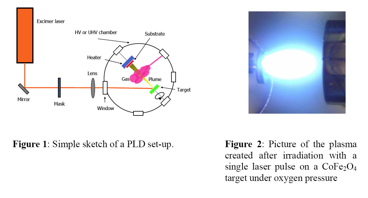
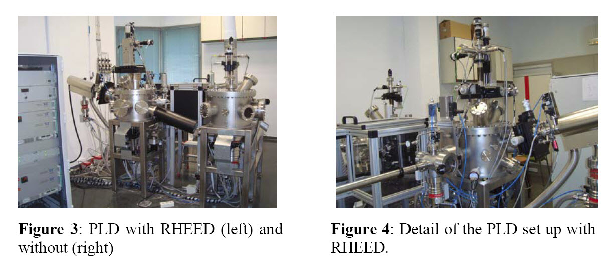
PLD is a physical vapour deposition technique that uses ultraviolet laser radiation to vaporize material that is transferred to the substrate. The plot in Figure 1 is a sketch illustrating a PLD set-up. The pulsed beam of an ultraviolet laser (usually an excimer) is focused on a ceramic target placed in a vacuum chamber. The combination of pulsed irradiation, high photon energy, and high energy density can cause the ablation of the material. Ablation refers to the etching and emission of material under conditions totally out of the equilibrium. The plasma created expands fast along the perpendicular direction of the target (see the photography in Figure 2). A substrate is placed front the target, and inert or reactive gases are usually introduced during the deposition process.
The technique is very suitable for oxides, and compared with other techniques is particularly useful to obtain films with complex stoichiometry and to grow epitaxial films and heterostructures. Moreover, PLD is highly versatile to optimize the deposition conditions of new materials, and the films can be grown in relatively fast processes. These characteristics favour the use of the technique by research groups having interest in different materials.
Equipment
The Laboratory owns two PLD deposition systems (see photographs in Figures 3 and 4) and the beam of an excimer laser can be directed to each of them (see the sketch in Figure 5). The systems were fabricated by Twente Solid State Technology. The two multilayers in a single process. Both substrates and targets can be loaded via the load lock. The base pressure in both PLD systems is below 10-8 mbar, and the substrate heaters permit high deposition temperature (up to 900 ºC) under oxygen or argon pressure. One of the chambers integrates a reflection high energy electron diffraction (RHEED) system for growth dynamic studies and real-time control of the deposition. It uses a 35 kV electron gun and two-differential vacuum stages that allow monitoring the growth under high-pressure up to 0.5 mbar. As an example, Figure 6 shows the variation of the RHEED specular spot intensity during layer-by-layer growth of around 4 monolayer La0.66Sr0.33MnO3 film on SrTiO3(001), with the patterns of substrate and film.
In 2012, the PLD chambers will be integrated in a cluster-like structure, including distribution and storage chambers, and metallization chamber with several sputtering sources. The storage chamber will permit the connection of a UHV vacuum suitcase to transfer Omicron-type plates, also compatible with the PLD set ups.
 Figure 5: Sketch of the PLD laboratory at ICMAB. In 2012 the PLD chambers will be integrated in a cluster with other chambers.
- Figure 6: RHEED monitoring of layer-by-layer growth of around 4 monolayer La0.66Sr0.33MnO3 film on SrTiO3(001).
- Figure 6: Patterns of substrate and film
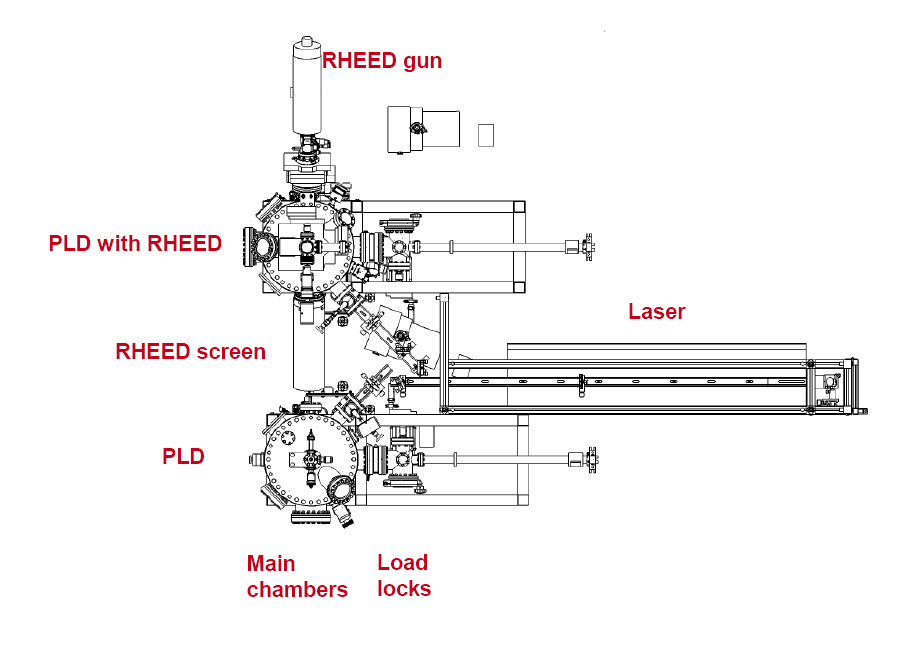 Figure 5: Sketch of the PLD laboratory at ICMAB. In 2012 the PLD chambers will be integrated in a cluster with other chambers.
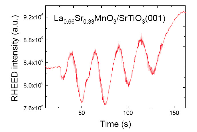 Figure 6: RHEED monitoring of layer-by-layer growth of around 4 monolayer La0.66Sr0.33MnO3 film on SrTiO3(001).
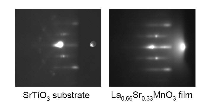 Figure 6: Patterns of substrate and film
Our publications that include RHEED results
- F. Sánchez, R. Bachelet, P. de Coux, B. Warot-Fonrose, V. Skumryev, L. Tarnawska, P. Zaumseil, T. Schroeder, J. Fontcuberta
Domain matching epitaxy of ferrimagnetic CoFe2O4 thin films on Sc2O3/Si(111)
Applied Physics Letters 99, 211910 (2011) - R. Bachelet, P. de Coux, B. Warot-Fonrose, V. Skumryev, J. Fontcuberta, F. Sánchez
CoFe2O4/buffer layer ultrathin heterostructures on Si(001)
Journal of Applied Physics 110, 086102 (RC) (2011) - R. Bachelet, C. Ocal, L. Garzón, J. Fontcuberta, F. Sánchez
Conducted growth of SrRuO3 nanodot arrays on self-ordered La0.18Sr0.82Al0.59Ta0.41O3(001) surfaces
Applied Physics Letters 99, 051914 (2011) - R. Bachelet, P. de Coux, B. Warot-Fonrose, V. Skumryev, J. Fontcuberta, F. Sánchez
Flat epitaxial ferromagnetic CoFe2O4 films on buffered Si(001)
Thin Solid Films 519, 5726-5729 (2011) - R. Bachelet, D. Pesquera, G. Herranz, F. Sánchez, J. Fontcuberta
Persistent two-dimensional growth of (110) manganite films
Applied Physics Letters 97, 121904 (2010)

Electron Microscopy
Electron microscopy is a fast-evolving field and new exciting findings can be expected with the advent of recent developments such as spherical aberration correction, monochromated guns or new advances in magnetic imaging techniques such as electron magnetic circular dichroism at the nanometer scale, just to name a few. Real space probes capable of looking at matter with atomic resolution and single atom sensitivity are a reality that provides new googles we can use to look into the nanoworld, and beyond.
Some of challenges in materials physics can only be studied using advanced electron microscopy techniques. Imaging and spectroscopy in the aberration corrected scanning transmission microscope can unravel point defects that trigger a dilute magnetic behavior in superconducting films, help to understand the role of oxygen vacancies and strain in cobaltite thin films, identify spin state superlattices or surface magnetism in nanoparticles, and can also achieve the mapping of minimal lattice distortions associated with light O atoms near interfaces that change drastically the macroscopic properties of complex heterostructures. The combination of electron microscopy, spectroscopy and atomic-scale quantum mechanical calculations represents a unique and extremely powerful tool for resolving the complex mysteries of materials.